
Retired & Halted Prototype Boards
Legacy board iterations, superseded hardware designs, and paused development projects
Earlier design iterations, paused projects, and retired board revisions are maintained here for full design transparency, hardware revision reference, and development history. These designs have either been superseded by improved carrier boards, split into specialized modular units, or halted due to economic or prioritization factors.
⏸️ Halted Designs
Boards that are not prioritised or not economical to produce at present.
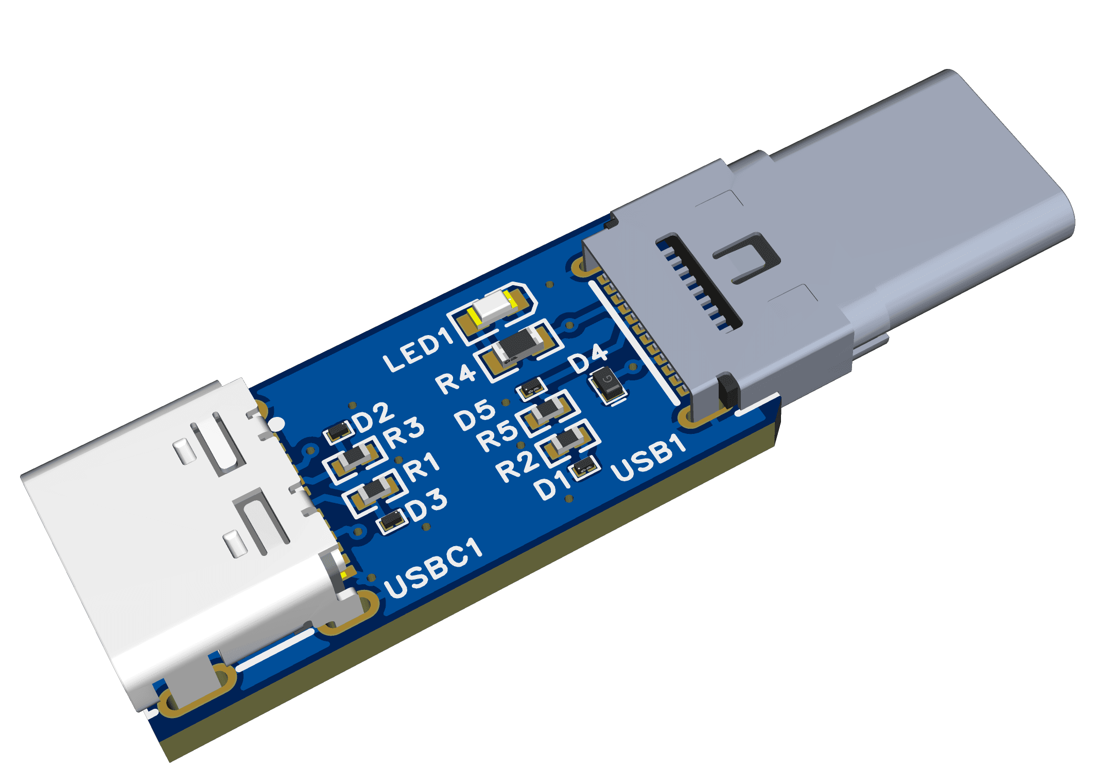
USB-C Data Shield
A hardware-level data blocker that allows safer device charging from public or untrusted USB-C ports by physically isolating all data lines.
Why This Board Exists
Circuit & Layout Details
- Physical Data Isolation: Complete severance of USB-C high-speed and legacy data lines (D+, D−, TX+, TX−, RX+, RX−, SBU1, SBU2). There are no copper trace connections for these pins between the input and output connector footprints.
- Basic Charging Support: Uses dedicated 5.1 kΩ pull-down resistors (Rd) on the Configuration Channel (CC) lines. This advertises a standard UFP (Upstream Facing Port) role to the power source, enabling basic 5 V charging without Power Delivery (PD).
- No PD Negotiation: Intentionally bypasses USB Power Delivery (PD) controllers to ensure the voltage never climbs above a baseline 5 V, reducing exposure to unexpected high-voltage negotiation or protocol-level behaviour.
- Power Protection: Includes transient protection on the VBUS rail to help clamp voltage spikes and ESD events on the power path.
📦 Retired & Replaced Boards
Earlier design iterations that have been superseded by improved carrier boards or split into specialized modular units.
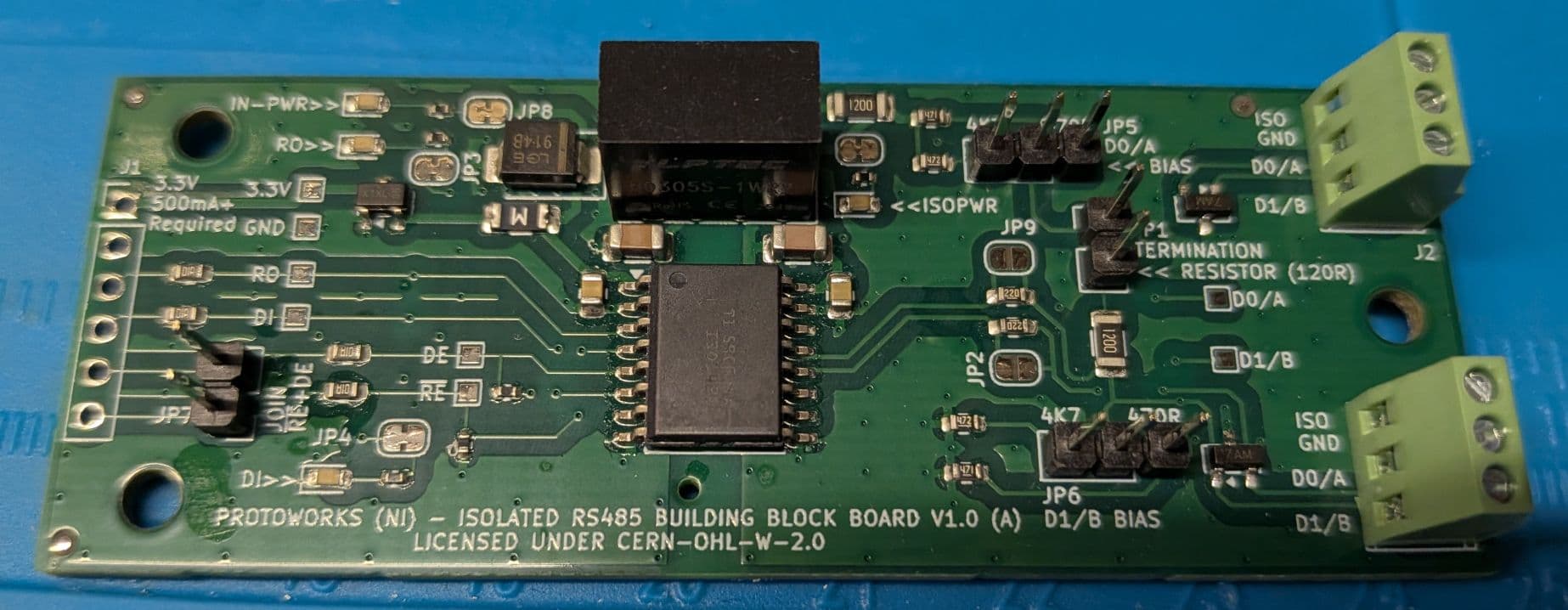
RS485 Isolated Breakout Board
An isolated differential serial interface designed to provide galvanic isolation between the host controller and the RS485 communication bus for noise immunity and ground loop prevention.
Why This Board Exists
Circuit & Layout Details
- Galvanic Isolation: Galvanically isolates the logic-side host controller from the RS485 cable side using an isolated RS485 transceiver and separate logic and isolated ground areas.
- Isolated Power Delivery: Employs an onboard isolated DC-DC converter powered from the host logic supply to generate isolated 3.3 V for the bus-side transceiver circuitry.
- Input Protection: Features a resettable PPTC fuse (500 mA hold current) and a clamp diode on the logic-side 3.3 V supply to protect the board from power supply faults or downstream shorts.
- Bus Configuration: Includes onboard jumper-selectable 120 Ω bus termination and selectable A/B bus biasing networks to set the defined idle state of the bus.
- Direction Control: Features configurable jumpers to link the DE and /RE lines, allowing a single host GPIO to manage half-duplex transmit and receive state transitions.
- Physical Layout: Promotes clear electrical isolation boundaries with 2.54 mm headers on the logic side and robust screw terminals for the isolated RS485 bus connections.
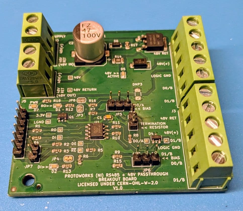
RS485 Breakout with 48 V Passthrough Board
A straightforward non-isolated differential serial interface for testing robust communication over longer cable runs, featuring a 48 V power passthrough option.
Why This Board Exists
Circuit & Layout Details
- Transceiver: Based on the 3.3 V MaxLinear SP3485EN differential transceiver.
- Bus Configuration: Includes onboard jumper-selectable 120 Ω bus termination and selectable bus biasing using either stronger 1 kΩ or weaker 4.7 kΩ resistors to establish the idle state of the bus.
- Direction Control: A single jumper links the DE and /RE lines, allowing a single microcontroller GPIO to control the transmit/receive state.
- 48 V Passthrough: Routes a high-voltage auxiliary supply across nodes for distributed systems. The 48 V path is protected by a conventional SMD fuse, a TVS diode, and P-channel MOSFET reverse-polarity protection.
- Layout Separation: Non-isolated design, but laid out with physically distinct 48 V return and logic ground regions to prevent heavy current return loops from interfering with low-voltage logic references.